

Introduction-
Consider your smartphone a little. It is literally a supercomputer in your pocket, powered by artificial intelligence, streaming high-definition video, and connecting you to the world, and barely warming up. How is this possible? This solution is in part based on 3D chip stacking.
We have been constructing computer chips in the same fashion that we might lay tiles on the floor, by sprinkling all of that over a silicon surface over the last few decades. This two-dimensional process worked so well, as it rode the tide of the Moore Law with engineers adding more and more transistors to every chip. But there is a point; we are hitting walls here. Not figurative ones- real physical boundaries. When you reduce features to less than 3 nanometers (a fourth the thickness of 15 atoms), heat becomes almost uncontrollable, and the wee wires interconnecting it all begin to create severe delays.
So, what did engineers do? They looked up.
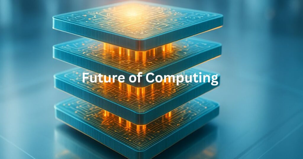
3D chip stacking. is literally that: it does not involve laying out components on a flat thermal conductive surface, but rather vertically, in a tower-like structure. This ostensibly straightforward change of mindset is transforming not only the AI systems that drive ChatGPT but also the memory in your laptop, data centers and self-driving vehicles.
This article is going to examine the principles of 3D chip stacking, the reasons why it is important, and where it is leading. As a curious student, a technology enthusiast or someone, working in the industry, I want to show you not only the what of this technology, but the why and how, in a way that makes you feel not as you would in reading a textbook, that you are having a conversation with someone who is truly excited to tell you about something interesting.
Understanding 3D Chip Stacking: Building Upward Instead of Outward
The Core Concept: Silicon Skyscraper
Let me paint you a picture. Suppose that you are a city planner and you are out of space. There are two options: to expand the city into the periphery with the additional cost of more roads and a longer travel time between districts, or to construct vertically by erecting high-rise buildings where people can easily travel between floors using elevators, as in 3D chip stacking.
The technology is also known as 3D integrated circuits, or 3D ICs. It vertically integrates several layers of semiconductor dies (individual silicon pieces containing circuits) into a single compact package. Rather than using long horizontal wires over the chip surface (which causes delays and power loss) to connect components, it uses short vertical circuits called “vias” that run through the silicon.
The physics makes the advantages clear. In conventional 2D chips, squeezing in more transistors lengthens the wires, like congested highways, which delays signals, wastes energy, builds heat, and slows the system. Stacking chips vertically allows multiple chips in the space of one, reducing the distance signals must travel.
The evolution of Chip Packaging: How We Got Here.
The history of 3D stacking did not begin yesterday. It has been simmering for decades like an oven, and with every generation of engineers, the knowledge of the predecessors is enhanced.
In the 1990s, System-on-chip (SoC) designs were produced, including logic circuitry, memory, and analog functions on a monolithic chip (a single silicon die). As systems became more complex, there was a need for more. In the late 1990s and early 2000s, Multi-Chip Modules (MCMs) emerged—these packages contained multiple dies placed inside one chip package, like adjacent houses on a block.
Then followed 2.5D architectures, in which a so-called silicon interposer (a passive, flat piece of silicon acting as a bridge) was used. This allowed several chips to be mounted on top of the interposer and connected with very short connections. This was evident in the early high-performance graphics processors, in which speed was of paramount importance.
However, the breakthrough came in the 2010s in the form of Through-Silicon Vias or TSVs. These are small vertical holes, such as elevators bored through the layers of silicon, and thus can be stacked vertically. In 2013, Samsung made history and introduced the first commercial 3D-stacked DRAM (Dynamic Random-Access Memory, used as fast working memory in computers), and later developed it to become High Bandwidth Memory (HBM)—the very fast memory used in modern AI accelerators.
And the impetus so prodigal. The 3D stacked chips market was estimated to be 2.08 billion dollars in the year 2025, and industry analysts estimate the market to be almost 8 billion in the year 2032- that is a growth rate of more than 21 percent. What is fueling this catapulting development? The insatiable ambitions of artificial intelligence and high-performance computing.
The Technology behind the Magic: How It actually works.
At this point, we shall dive into the details of the communication process between the layers in these chips. There exist three technologies in play: Through-Silicon Vias (TSVs), micro-bumps, and hybrid bonding.
The horses of 3D stacking are Through-Silicon Vias (TSVs). Imagine that they are small vertical conduits stocked with conductive materials such as copper. They literally drill holes into the silicon and provide direct conduction paths of both electrical power and electrical signals between layers. It is as though you were drilling elevator shafts through a building, and it is on a microscopic scale.
Micro-bumps are tiny solder joints, in other words, tiny bridges made of metal that physically connect one die to another. They can be depended upon and they are comparatively easy to produce, but they are limited in size.
The most advanced and latest method is hybrid bonding. It does not solder its connections; instead, it bonds the copper connection points and the insulating oxide layers between chips at the atomic scale. Think of two articles of glass, which you are to press together–they will stick together without adhesive. With silicon, a similar thing is attained in hybrid bonding that forms extremely close and efficient connections.
Consider a 3D stacked chip where the logic processor, the brain, is on the lower level, and memory is stacked above. In a 2D architecture, the processor issues data requests over long horizontal wires, taking microseconds. In 3D stacking, requests flow vertically using TSVs, reducing latency to nanoseconds—a thousand times faster!
The flow is two-way; up and down, just like communication between floors of a building. Engineers have in the meantime, devised smart methods of moving heat and signals via embedded channels, and have developed a small ecosystem where layers actually cooperate as a single system.
The Technologies Making It Possible: Engineering Marvels at Microscopic Scales
Through-Silicon Vias: Drilling Through Silicon
TSVs are enormous engineering marvels. Suppose you could punch a hole through a silicon wafer a little more than a human hair thick, and ten times as deep as the wafer itself, and then fill it up to the brim with metal. We are doing that on an industrial scale.
It begins with deep reactive ion etching, which is a process that employs a plasma to etch these high-aspect-ratio holes (down to depth-to-width ratios of 10:1). Next, we have the electroplating, where we carefully insert the metals, such as copper or tungsten, into the vias. Lastly, it is polished by a chemical mechanical method that smooths it all to produce an absolutely flat surface.
However, the problem is as follows: when silicon and copper are heated, their rate of expansion is different. It is as though attempting to construct a tower with bricks that are not growing at the same rate, something will snap at some point. To avoid this, they put a barrier layer on the surface of the design, which can be composed of such a material as tantalum, serving to buffer the copper and not allowing it to be diffused into the silicon, and dealing with the thermal stress.
Nevertheless, contemporary TSVs are highly advanced, with the distance between the vias (pitch) as narrow as 10 micrometers in advanced chips. The main limitations? Cost–the process of fabrication is complicated, and the fabrications may contain defects such as voids, misalignment, or that interminable thermal expansion nonconformance. Nevertheless, TSVs are completely indispensable to 3D stacking.
Micro-Bumps and Hybrid Bonding: Bonding the Layers.
As far as literally joining dies together, there are two approaches, and they reflect rather different philosophies.
Micro-bumps make connections between chips with small solder alloys (such as tin-silver alloys). These connections operate at frequencies of approximately 40-50 micrometers (the distance between bumps known as pitch) and are quite mature and not expensive. Imagine them as tiny solder balls that melt and solidify with heat. They can be used in many applications, but have scaling issues: as we make them smaller, problems such as electro migration (where electrical current causes metal atoms to move within the wire) and voids (small empty spaces that can form under the connection, which are then filled with a material called under fill) can arise.
On the contrary, hybrid bonding is the newcomer on the block, and it is impressive. It does not employ solder and bonds copper pads and oxide dielectrics directly at the atomic scale. The result? Bonds made at lower levels, less than 10 micrometers, i.e., less than sub-10um, which is much smaller than the capability of micro-bumps.
The figures speak for themselves: hybrid bonding yields approximately 15-fold greater interconnect density and an approximate 3-fold more efficient energy consumption, about 15 times better than micro-bumps. It is able to reduce electrical resistance by up to 81 percent of conventional 2D designs in timing-critical pathways. That is a direct translation into less power-consuming chips.
The catch? The surfaces of the wafer require an unbelievably clean, flat surface. Hybrid bonding requires, literally, an atomic-level smoothness. Any dirt or coarseness destroys the connection. Micro-bumps are, therefore, the best choice when the cost of modules matters and good enough is, well, good enough; however, when it comes to ultra-fast AI accelerators and every nanosecond and mill watt matters, hybrid bonding is the market leader.
Thermal Cooling: Innovations in Thermal Management.
This is a pain to hear on the subject of 3D stacking: as you squeeze more electronics into a smaller space, you are concentrating the heat. Actually, the heat density may be five times that of 2D designs. Layers between the others, like sandwiches, cannot easily lose their heat; it is as though putting on several winter coats on a hot day. This entrapment of heat has the capacity to cause thermal runaway, in which an increase in temperature increases the speed of the issues, causing failures.
What then do engineers do about this? There were certain genuinely clever things.
One of the most promising methods is microfluidic cooling. Think of cutting little grooves into the silicon layers and pumping some of the cooling fluid through the grooves–a little micro-plumbing system constructed right into the chip itself. Practically, it is no longer just science fiction, with Microsoft demonstrating this breakthrough in 2025 with its AI chips.
Thermal TSVs do not do this. These vias are also filled with materials that are highly conductive to heat, and in effect, they form chimneys that allow hot air (or in this case, heat energy) to escape the inner layers to the outer surfaces, where it can be cooled.
Graphene heat spreaders take advantage of the amazing thermal capabilities of a one-atom-thick sheet of carbon, which is an excellent heat conductor, nearly as efficient as diamond. These spreaders should be placed strategically in the stack to spread heat at a more uniform rate.
Studies by MIT and others have verified these methods in actual test chips with results indicating that they are able to down-regulate the temperature of the hotpot by 50 °C or even higher. The difference between a chip, which cannot run as fast as it could go without breaking down, and one that can run faster and stay reliable is that. Naturally, such cooling solutions will complicate and increase the cost; however, in the case of applications with high performance, it is a must.
Advanced Materials: The Unsung Heroes.
In addition to the headline technologies, the great ecosystem of advanced materials that enable 3D stacking also exists.
Silicon interposers are used as passive bridges in 2.5D and 3D connections, which are a solid platform with highly accurate wiring patterns.
High-k dielectric materials, such as hafnium oxide, with high dielectric constants, insulate such fine-pitch vias without consuming a lot of space.
Novel adhesives are also important. Polymers with low modulus can be used to inhibit warpage (when chips bend under thermal stress), and adhesives containing carbon nanotubes can be used to increase thermal conductivity, and hence to conduct heat where it is required.
These materials also allow heterogeneous integration = combining and matching other kinds of semiconductors. Need silicon logic with gallium nitride in radio frequency applications? That is possible with advanced packaging materials, which allow us to construct systems that would otherwise not be possible using other traditional methods.
Why 3D Stacking Matters: The Compelling Advantages
Speed That Makes a Difference
Let’s talk about distance. A signal in a 2D conventional chip could take several millimeters to get to the destination part of the chip. The same trip, in a 3D stack, is only a few micrometers, literally a thousand times shorter.
Why does this matter? Although signals travel rapidly, they do not travel at infinitesimal speed, and even when the speed is that of light, delays due to the signal’s speed will accumulate when you are operating at gigahertz frequencies. 3D stacking reduces signal propagation delays dramatically by allowing a reduction in distance by 80 percent or more. It translates to increased clock speed and, more importantly, reduced time wastage on waiting for data.
Consider Take High Bandwidth Memory (HBM). The modern HBM stacks are capable of providing 1.2 terabytes per second bandwidth. In order to make that perspective, that is approximately 300 full-length HD movies within one second. This bandwidth is of paramount importance in the case of AI accelerators, the special processors that execute large language models and neural networks. GPUs are highly powerful, yet they are normally data hungry. HBM solves that bottleneck.
Power Efficiency: Getting More, Spending Less.
And here is the surprising fact to you: shorter wires do not merely make the chips faster, but make them more energy-efficient as well.
Parasitic capacitance is present in every wire–it is a kind of tiny capacitor that must be charged and discharged with each switching of a signal. The longer the wire, the more energy is wasted. With 3D stacking, the dynamic power consumption can be cut by 30-50% by dramatically decreasing interconnects. That is not energy that is becoming heat, that is not energy that is depleting your battery, and that is not energy that is filling your electricity bill.
In the case of battery-powered gadgets, such as smartphones, tablets, and wearables, this efficiency is directly converted into an extended working period. In the case of data centers, it translates to a reduced cooling cost and reduced carbon footprint. It is one of those few win-win scenarios in which a better performance actually consumes less energy.
Packing More into Less: Miniaturization and Density.
Density is one of the most material advantages of 3D stacking. With the upwards design, we will be able to fit approximately five times the number of transistors onto the same physical area as a 2D circuit.
What does this enable? Thinner, lighter wearables. Smartphones that were able to do what would have taken a decade to be done by desktop computers. Dense server racks in the data center, i.e. higher computing power per square foot of costly real estate.
In the case of Internet of Things (IoT) devices, this is disruptive. Consider the sensors that must contain processing capabilities, memory, communication networks, and power control all in a package less than a few millimeters across. 3D stacking becomes useful.
Mix and Match: Heterogeneous Integration.
The following is one of my most favored features of 3D stacking: it allows us to create hybrid systems in a manner that was previously impossible or not viable.
Various circuits have different best manufacturing processes. State-of-the-art logic (the CPUs and GPUs) enjoys the virtue of the tiniest conceivable transistors – imagine that is 3 nanometers or so. However, at large nodes, such as 28 nanometers, analog circuits, sensors, and some kinds of memory all work well (and are significantly cheaper).
Under a standard 2D design, all the components in the chip have to be produced through the same process. It is a waste of time, the same way as having to fill a car with premium gas instead of regular, which works well. 3D stacking is a game-changer. You are able to have your high-performance 3nm logic on one layer and a cost-effective 28nm analog circuit on the other, and optimize each to its purpose. Put them one atop another, and you have system-level performance without spending money unnecessarily on making everything bleeding-edge.
This freedom also applies to entirely dissimilar materials as well, such as silicon to digital logic, gallium nitride to power electronics, or dedicated sensor materials, all of which are packaged into a single package.
The Challenges We’re Still Solving
Naturally, there are also challenges in every field of every technology. The technology of 3D chip stacking is incredibly potent, yet it is also accompanied by challenges that are real, and engineers are trying to address them.
The Heat Issue: Thermal Hoteliers.
This has been mentioned above, but it should be underscored that thermal management is by far the largest issue in 3D stacking.
With a tight assembly of layers of active electronics, heat can be trapped in the deepest layers, as the warmth of the middle of a blanket. These hot inner layers under heavy load may get to 150 °C, which is hot enough to become unreliable. Electromigration, in which current literally drags metal atoms about, increases in speed at high temperatures, leading to the eventual breakdown of wires.
Although we have mentioned above such innovations as microfluidic cooling, thermal TSVs, and heat spreaders, which contribute greatly to this purpose, they are expensive and complicated. It is a constant game of juggling: how to extract the most out of it and how to keep the temperatures down. In certain applications, especially in mobile devices where there are no cooling choices, thermal considerations will constrain the stacking aggressiveness.
Complexity in Manufacturing: Accuracy on the Microscopic Level.
The construction of a 3D stacked chip is exceptionally complicated. The different layers will have to be aligned with the ones on the top and bottom within a sub-micron, which is a precision of a millionth of a meter. The bonding process, micro-bump process, or hybrid bonding of process should be almost flawless.
This accuracy needs complex lithography and a very strict control of processes. Defects can be created by any contamination, any even minimal misalignment, any gap in the connections. And since we are piling up many layers, problems have a multiplier effect; a little trouble on one layer can be experienced on all the layers above it.
The result? The production of a 3D stacked chip is more difficult compared to the production of a 2D chip, and it involves the use of special equipment, knowledge, and quality assurance.
Cost and Yield: The Economic Reality.
This is the bottom line–literally. Preliminary expenditure of 3D stacked chips is usually two to three times more than the equivalent 2D designs. That accuracy, all of those extra process steps, all the specialized materials, they are money.
In addition, yields (percentage of chips that behave correctly) are also lower. In simple 2-layer stacks, yields can be very good, whereas in complicated 4 or more-layer stacks, they can fall to 80 or less. Why? Because errors compound. Assuming that every layer has a 95% yield (that is quite good!), five layers stacked together would only yield you about 81% in the stack.
This economic fact implies that 3D stacking is prudent in the high-value applications, where the benefits of performance outweigh the cost premium, which includes AI accelerators, high-end processors, and high-quality memory. The costs will reduce as the technology is more mature and the volumes are higher; however, at present it is a premium solution.
Testing and Repair: When Things Go Wrong.
This is a tricky issue because, once you have stacked and bonded more than a few dies into a stack, how can you test the inner layers? With a conventional chip, you may probe any circuit prior to packaging. However, in a 3D stack, the central layers are literally covered by others.
Testing takes either detailed self-test circuits (which would add space and complexity) or destructive probing (neither feasible nor economic to do in production). And even when something goes wrong? It is very hard or impossible to repair. You can not exactly disassemble the stack, repair one of the layers, and reassemble it.
The solution is known- good die screening: testing every layer exhaustively before stacking. However, this is time-consuming and costly and not always ideal. Other defects do not manifest until after being stacked by thermal or mechanical stress. The industry is yet to tackle it in a better manner.
The Areas of 3D Stacking that are transforming the world today.
Nevertheless, 3D chip stacking has already been implemented in hundreds of real-world applications, with amazing effects of performance change being experienced.
Memory Technology: Denser, Faster Storage.
Perhaps the most developed use of 3D stacking is in memory technology.
The poster child of the success of 3D stacking is High Bandwidth Memory (HBM). The most recent generation is the HBM3E, which is stacked vertically with more than one DRAM die, with a record data rate of 9.6 gigabits per second per pin. NVIDIA flagship AI GPUs are powered by this memory, as it would be heavily bottlenecked without it. You come to a point of training a large language model with hundreds of billions of parameters, and you need to feed the processor with large volumes of data at any given time- HBM is what enables that.
3D NAND Flash goes further with stacking, with certain chips stacking 200 or more memory cell layers. This is the technology within the current solid-state drives (SSDs) that allows storage of petabytes to be stored in small form factors. The fast SSD of your laptop? Most likely, it has 3D NAND, which has an incredible amount of capacity in a small size.
Mobile and Consumer Electronics: Power in Your Pocket.
The mobile sector has eagerly pursued 3D stacking due to the obvious reasons; smartphones require optimum performance in the least amount of space and use little battery power.
The 2025 smartphones based on Qualcomm Snapdragon processors apply 3D stacking to combine CPU, GPU, AI accelerators, and memory in exceptionally small packages. It allows things that appeared to be science fiction only a few years ago, such as real-time augmented reality, immediate language translation, and advanced computational photography.
In the case of AR and VR headsets, space and power are at zero premiums; 3D stacking has increased rendering performance by at least 40 percent and ensured the devices stay cool enough to be comfortable to wear. That is the distinction between the cumbersome prototypes and products that the consumers can use.
Data Centers and AI: The Backbone of the Modern Computing.
3D stacking is transforming the performance of data centers that are serving an entire universe of web searches, AI chatbots, and much more.
The EPYC server CPUs of AMD incorporate 3D V-Cache- the extra layers of cache memory placed at the top of the processor cores. The technology is approximately 15 times faster in executing machine learning workloads and is a faster way to train and perform more efficient inference of AI applications. A 15 percent increase is enormous, especially when you have thousands of servers to take into consideration.
Exascale computing -systems with the capability of a quintillion (a billion billion) calculations per second are also being made possible by these architectures. Climate modeling and drug discovery are only a few of the issues that such systems are addressing that could not have been previously done.
Automotive and Edge Computing: Solid Performance Where It Matters.
In your car, particularly in those with advanced driver assistance systems (ADAS), there are probably stacked 3D Chips that are operating behind the scenes.
The computational density of self-driving systems must be able to process dozens of inputs at the same time, integrating the information provided by cameras, radar, lidar, and ultrasonic sensors, and must be as robust as the automotive industry demands. 3D stacking allows the computational density to fulfill these goals and requirements simultaneously.
These chips must also be compatible with extreme weather: from -40 °C winters to hot dashboards of 125 °C. Modern stacks of 3D are planned to have this thermal stability so that your car can be safe no matter the weather.
What’s Happening Now: Industry Trends and Innovations
The 3D chip stacking is developing at a very high rate. So, how about the activities of the big players and the direction of the research?
The Leaders in the Industry and their strategies.
The Foveros technology pioneered by Intel allows logic-on-logic stacking, or more simply put, laying processing layers on top of one another. This is demonstrated by their Lunar Lake CPUs introduced in 2025, where high-performance cores and efficient cores are combined in a vertically stacked design.
AMD has rocked 3D V-Cache, which entails adding more cache memory on top of their processor cores. In games, this has increased the performance of its Ryzen processors by approximately 20% – a big gain considering that this is the change that was fairly simple to make.
Taiwan Semiconductor Manufacturing Company (TSMC) is the largest chip manufacturer in the world that has come up with SoIC (System-on-Integrated-Chip), which incorporates the hybrid bonding. This technology is available in the M4 chip created by Apple, which has been able to combine performance and efficiency in a manner that has revolutionized the expectations of laptop computers.
Samsung and SK Hynix are struggling to dominate the HBM market. The HBM4 developed by Samsung will be available in 2025 with a maximum bandwidth of 1.4 terabytes per second in AI applications. SK Hynix entered the market in April 2025 with competitive products that led to the creation of healthy competition.
The next direction Research Is Moving.
Researchers are looking even further with more ambitious methods, other than commercial products.
Monolithic 3D Integration is an integration method that seeks to manufacture transistors in layers and hang them one upon another over the top, instead of stacking entire dies. This might allow even a closer integration, but the production issues are vast.
The wafer-to-wafer bonding is also under development to scale the production, and this may reduce the cost and enhance the yield since the entire wafer is bonded together and then sliced into separate chips.
The architectures designed by AI to the ground up are 3D stacked, in which evaluations of features such as dynamically assigned cache are designed that relocates down and up the stack depending on the workload requirements.
Working Together: Standards and Collaboration.
To achieve the full potential of 3D stacking, the industry requires standardized practices and common standards.
Interfaces to HBM and other types of stacked memories are being defined by organizations such as JEDEC (which standardizes memory technologies) to ensure that the chips of different manufacturers can be compatible.
IEEE (the Institute of Electrical and Electronics Engineers), is progressing testing protocols of 3D structures specifically so that the industry can overcome the difficult testing and reliability problems we have identified above.
Such working arrangements will help make 3D stacking an ecosystem as it grows, not a set of proprietary strategies, making it more widely adopted and more innovative.
Perspective: The Future of 3D Stacking.
Where is all this heading? And now, as we look into the future, not with speculation, but with a reasonable forecast, with the projections we have at any moment.
A.I. and Quantum Computing: The Next Frontiers.
The artificial intelligence is starving–starving with processing power, starving with bandwidth, starving with energy efficiency. 3D stacking is well placed to satisfy these cravings.
The AI models of the next generation will include trillion-parameter networks– not GPT-4 and much larger. These models consume large amounts of data and massive parallelism to run, so 3D architectures that co-locate processing and memory can deliver both of them, and today, almost magical AI capabilities.
Quantum computing brings other, but equally thrilling opportunities. Quantum bits (qubits) demand high levels of error correction, and this necessitates arrays of aiding classical circuits as densely as possible. 3D stacking may enable quantum computers to be another deep circuit that can be densely implemented.
The Vision: True 3D System-on-Chip.
Suppose a chip in which compute cores, memory hierarchies, I/O interfaces, and specialized accelerators have been vertically integrated into one 3D structure-a real 3D System-on-Chip (3D-SoC).
The latency between inter-component communication could be cut almost to zero in such systems, allowing completely new computational paradigms. In the case of edge AI, or intelligence implemented on devices, not the cloud, this might imply microsecond or micro-millisecond responsiveness of autonomous systems.
We are not that far, but the basic technologies are being developed today. This vision has been made simple and engineers all over the world are striving to make it a reality.
Sustainability: Constructing a Greener Future.
The following is something that is frequently neglected: 3D stacking can be used to solve the environmental impact of computing.
Cuts in power consumption: 3D chip power consumption can be 30-50 per cent lower than on a comparable 2D design, which in turn can decrease the energy use of data centres by 20 per cent or more, as well as carbon emissions. That is a big contribution to the sustainability objectives.
In addition, the industry is also considering recyclable packaging materials and manufacturing processes that are more environmentally friendly. With improved performance and reduced environmental effects, 3D stacking will not only be technologically superior, but also responsible for
the environment as we continue scaling these technologies to 2030 and beyond.
Conclusion: A Vertical Leap Forward.
3D chip stacking is one of those few inventions that has altered the basic technology architecture. It is not a gradual advancement; it is a paradigm change.
It is by going upwards, rather than outwards, that we have discovered how to beat the physical constraints that were halting the advancement in semiconductor design. We have gotten density, speed, and efficiency that is not possible with the traditional 2D approaches. It is 3D stacking that is enabling the AI systems redefining our world, the future quantum computers, the smartphones that are becoming even more powerful than supercomputers, the data centers that are accelerating our digital life-everything is possible with 3D stacking.
Yes, challenges remain. There must be innovation in the field of thermal management. The complexity of manufacturing requires accuracy and skills. Costs are still premium. Reliability and testing should be further considered. The path, however, is obvious: the further in the future the generation, the less difficult these issues are, the better the benefits, and the more extensive the applications.
With the future of computing at our fingertips, 3D chip stacking is a marvel of human resource, our capability of thinking outside the box when we are confronted with what might appear to be immeasurable challenges. It is a reminder that there are moments that you must look up as well, when you cannot go ahead.
The following generation of electronics will not be faster or smaller. It will be more intelligent, productive, and able than we can even think of at the moment. And at its base, which is literally speaking, will be this fine solution: constructing not only over silicon, but through it.
Visual Guides and Further Reading
Recommended Visuals:
- Comparative Diagram: A side-by-side illustration showing 2D planar chip layouts (with their long horizontal wires) contrasted with 3D stacks (featuring vertical TSVs), highlighting the dramatic reduction in interconnect length.
- Cross-Sectional View: A detailed schematic cutting through a multi-layer 3D chip, showing TSVs, micro-bumps, and hybrid bonds, with labels explaining each component’s function.
- Performance Timeline: A line chart tracking HBM bandwidth evolution from HBM2’s 256 GB/s in 2016 to HBM4’s projected 1.4 TB/s in 2025, illustrating the exponential gains enabled by advanced 3D stacking.
For Deeper Understanding:
- IEEE Spectrum regularly publishes accessible articles on TSV fabrication and semiconductor manufacturing.
- Nature Electronics offers rigorous peer-reviewed research on hybrid bonding and advanced packaging techniques.
- Semiconductor Engineering provides industry reports on thermal management solutions and practical implementation challenges.
- Company Whitepapers: TSMC’s technical papers on SoIC, Intel’s documentation on Foveros, AMD’s deep-dives on 3D V-Cache, and Samsung’s HBM technology briefs offer manufacturer perspectives on cutting-edge implementations.
These resources will take you beyond this introduction into the fascinating technical depths of 3D chip stacking, whether you’re studying it academically or implementing it professionally.